Sequence Detector Example
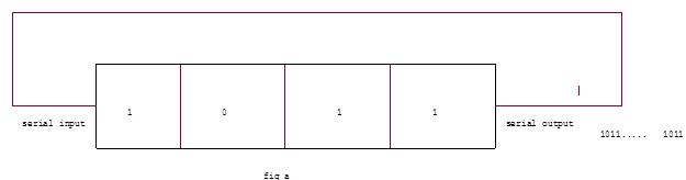
Sequence detector checks binary data bit stream and generates a signal when particular sequence is detected. The figure below presents the block diagram for sequence detector.Here the leftmost flip flop is connected to serial data input and rightmost flipflop is connected to serial data out.Clock is applied to transfer the data.Sequence generated doesn’t get lost as it is fed back again as serial input to fill the register.Thus for any n bit long sequence to be generated for this configuration we need to store the sequence in an n bit shift register.
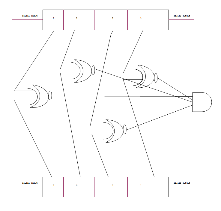
The above block diagram shows the sequence detection.br />br /> The circuit that can detect four bit binary sequence is shown in figure b below.It has one register to store binary word that we want to detect.Input data stream enters serial input and leaves from serial output.At every clock instant bitwise EX-NOR comparison is done .EX-NOR comparison gives logic 1 when both inputs are either high or low and final output is given by four input AND gate.This circuit can be used as programmable sequence detector where the word to be matched is stored in bottom register.For fixed sequence detector we can reduce hardware cost by removing bottom register and directly connect EX-NOR input to +VCC or GND depending on whether we want 1 or 0 to be detected at particular position. In the below figure the first two bits are mismatched in uppermost register ,now if input is 1 though serial input the sequence 1011 is matched in bottom register and hence output of AND gate is 1.Sequence detectors can be used in
- Phone unlocking
- Digital communication system
- Remote Control
So far we have learnt the basic mechanism behind sequence detector and how it works,now let us discuss about design part.Design part sarts with input and output specification and ends with circuit diagram having sequential and combinatorial parts.Input and output specifications can be converted into state transtion diagram or ASM chart followed by state synthesis table and excitation table for flip flops and then generating design through K-map.There are two approaches for state transtion diagram
- Moore model
- Mealy model
Here we will not go in details of these model as you can study from your text book or from internet but we will try to develop state transition diagram for 110 sequence detector using mealy model. State transition diagram is shown below
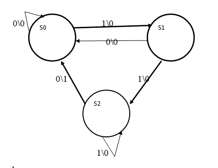
In the above diagram input and output is in X\Y format respectively.The circuit is intialized with state S0,if it receives X=0 it stays at S0 else goes to S1 that indicate that first bit is detected .At S1 if it receives 1 it goes to S2 and output remains is Y=0 in both cases.In state S1 if it receives X=0 then output Y=1 hence all the three bit pattern has been received,if at state S2 X=1 then the sequence received is 111 and output Y=0.
|
Here is the test bench for Sequence Detector
|
In the above verilog code we have defined states by equivalent binary number through keyword parameter.In the design part we have used three always block.First always block does state change at positive edge of clock when reset is low.Second always block decides what will be the next state when current input and current state is provided.Third always block decides the output for input and current state. In the testbench part we have tried to test the circuit by giving X=01011001101 for 110 detection.We can view the waveform as shown below
In the above waveform we will get y=1 at 60 sec and 100 sec according to testbench.Here input is from right if from left ,011 detection is performed.