Shift Register using verilog |
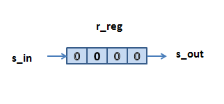
We will now consider a shift register. Our shift register has an s_in input entering on its left hand side. At each clock cycle, the content of the register shifts to the right and s_in enters into the leftmost bit or the MSB bit. The whole design also has and output that we are c calling s_out. At each clock cyccle the right most bit of the register comes out.
The picture shows the scheme of the shift register.
Here is the verilog implemmentation of shift register.
|
Explanation |
Initially the reg value of undefined and hence we have placed 4'bxxxx in its value.
Because of the assign statement
assign s_out = r_reg[0]; |
the initial value of s_reg[0] is also 0.
When the reset pulse is applied the r_reg becomes 0000 at the next rising edge of clock. Note that the period of the negative level of the reset sould last at least to the next rising edge of the clock
At this stage, the value of s_out also becomes 0 ( right after the rising edge of the clock).
Now the s_in value is supplied sometimes before the next rising edge of the clock. Now because of the assign statement
assign r_next = {s_in, r_reg[N-1:1]}; |
the wire r_next is driven by the value of s_in and [3:1] bits of r_reg.
And so, after the application of the s_in, at the next rising edge of the clock, the statement
r_reg <= r_next; |
in the always loop takes effect. which essentially results in updating the r_reg value with its value shifted to right and s_in coming in at its MSB.
The testbech for the Serial shift register
|
Exercizes
1. In test bench the shift register is instantiated with N=2. Verify that it behaves as expected. Repead the testbench and verification for N=4
2. Write the above code for left shift in place of right shift. The data now comes out of the MSB. The data enters from LSB.