PADS POWERPCB TUTORIAL
Routing the Board
If you have followed till the previous section, you should be able to do routing easily.
A Note on GRID and DRC checking - At this point you will like to set up smaller grid. The grid can be set using Setup-> Preferences -> Grids. A 5 mils grid is reasonable for routing.
The DRC rule can be set using Setup-> Preferences -> Design -> On-Line DRC. We will be doing this tutorial with DRC-Off.
Also set the minimum Display width from 10 to 1 using Setup -> Preference -> Global -> Minimum Display Width. Set it to 1.
Now let us do the routing. Click on Design Button
 and then click Add route button
  .
.
Click on the Inner Layer 3 and in the Plane Type - click Split/Mixed. Now click the Assign Nets. We want the VCC net to be assigned to the ground plane. So click on the VCC and click Add>>. Click OK.
Now click on Pin Number 1 of Diode D1 ( the end connected to Resistor). Now as you move the cursor, you should be able to see the routintg taking place. The default width is 6. If you want to change the width to, say 15 mils, you can do it on the fly with command w15.
Now let us assume we want to reach to resistor R1 by passing through the bottom layer. We will have to use via. Click left click somewhere while routing and the right click. Click on Via Type. You should see two vias - STANDARDVIA and MINVIA. For now the default is STANDARDVIA. Select the MINVIA. Click OK.
To Add a via just use command L4 ( Change to Layer 4). PADS will automatically addd a via and now you are in Layer 4. Keep routing till the resistor, till you reach to the pad to resistor and see a circle. Left Click to complete the routing.
Routing the Power Nets
The routing of the board is complete.The next step will be to check for DRC for clearance. Click on tools -> Verify Design -> Check Clearance -> Start.If there is any clearance related error, it will show up. You will have to clear all DRC errors before you proceed further.
You can see the above in a Flash movie in the following link. The Video will open in a new Page.
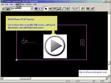
We will be covering Silkscreening, Board Dimensioning, Fabrication notes next.
If you like this tutorial, you may like to get the book Signal Integrity for PCB Designers